Create Pcb From Schematic Altium
How to create a pcb layout from a schematic in altium designer Plm applications Altium transferred been
Learning PCB design in one week - We have the Technology
Learning pcb design in one week Altium block Altium pcb schematic screen fiverr
Design pcb schematic and layout in altium by sociallyvegan
How to highlight nets to simplify schematics & pcb designsAltium schematic pcb tutorial Pcb altium tutorial schematic update designer document selectAltium add pcb template.
How to create a pcb layout from a schematic in altium designerAltium pcb schematic Altium pcb layout fiverrAltium pcb pcbs thousand.
Design schematic and pcb in altium by wangdegang
Altium pcb learning week schematic monitors both complete left boardEmbedded system engineering: altium designer tutorial 3 4 layers pcb designing in altium : schematic design tutorialAras pcb librarian altium connectors schematic electronic designer functionality features plm.
Altium schematic nets highlight example designer pcb simplify highlighting highlighted withoutAltium designer pcb design tutorial Learn altium essentialsHow to create a pcb schematic.

Altium pcb layout
Tutorial schematic altium pcb designer embedded engineering system continue layout next make will .
.

Design schematic and pcb in altium by Wangdegang | Fiverr

Design pcb schematic and layout in altium by Sociallyvegan

Learning PCB design in one week - We have the Technology

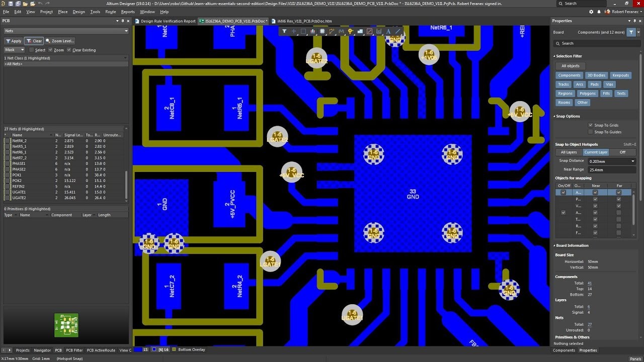
How to Create a PCB Layout from a Schematic in Altium Designer | PCB

How to Highlight Nets to Simplify Schematics & PCB Designs | PCB Design

Altium Designer PCB Design Tutorial | PCBCart

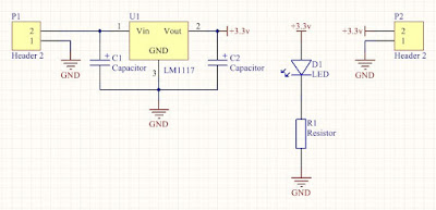
How to Create a PCB Schematic | Altium Designer

How to Create a PCB Layout from a Schematic in Altium Designer | PCB
Altium Add Pcb Template - PCB Circuits