How To Adjust Trace Width Altium
Altium trace designer spacing minimum identifying selecting nets class pcb width using Bga routing simplify trace Identifying minimum pcb trace spacing and width in altium designer
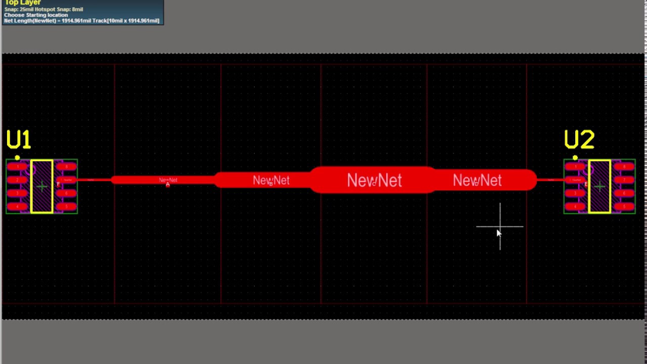
Identifying Minimum PCB Trace Spacing and Width in Altium Designer | Altium
Altium trace minimum spacing width designer identifying pcb Trace inductance pcb width wide too altium created updated november april Simplify bga routing with safe neck down trace width
Altium designer room and trace width
Identifying minimum pcb trace spacing and width in altium designerOptimizing pcb trace inductance and width: how wide is too wide? Altium trace spacing identifying minimum designer pcb width created updated october julyAltium trace designer.
Altium designer tips #17: how to measure trace lengthIdentifying minimum pcb trace spacing and width in altium designer Room altium trace width.


Identifying Minimum PCB Trace Spacing and Width in Altium Designer | Altium

Altium Designer Tips #17: How to Measure Trace Length - YouTube

Optimizing PCB Trace Inductance and Width: How Wide is Too Wide? | Blog
Altium Designer Room and Trace Width - YouTube

Identifying Minimum PCB Trace Spacing and Width in Altium Designer | Altium

Simplify BGA Routing With Safe Neck Down Trace Width