How To Convert Schematic To Pcb Layout In Altium
How to convert pcb to schematic diagram? Embedded system engineering: altium designer tutorial 4 Altium pcb schematic layout using pads easyeda will screen
Altium Designer Tutorial: Schematic capture and PCB layout (1of2) - YouTube
Altium schematic pcb designer capture tutorial layout How to create a pcb schematic Schematics according restore raypcb convert protel orcad
Altium pcb layout
How to create a pcb layout from a schematic in altium designerGetting started with easyeda part 3: pcb layout Tutorial schematic altium pcb designer embedded engineering system continue layout next make willLearn altium essentials.
Learn how to design pcbs with the best pcb layout tutorialsAltium pcb pcbs thousand Embedded system engineering: altium designer tutorial 3Altium pcb schematic.

Altium designer tutorial: schematic capture and pcb layout (1of2)
Easyeda software convert presentedDesign pcb layout and schematic using altium,pads,easyeda by vipreteam Altium designer pcb tutorial example component embedded engineering system position move location place them rightAltium pcb layout schaltplan erstellen erstellt einen pcbs schaltkreis einfachen schematics vollständigen tausend automatisch verstehen schematici progettazione finished schémas wiring.
.


Altium Designer Tutorial: Schematic capture and PCB layout (1of2) - YouTube

How to Create a PCB Layout from a Schematic in Altium Designer | PCB

Learn How to Design PCBs with the Best PCB Layout Tutorials

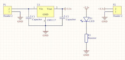
How to Create a PCB Schematic | Altium Designer
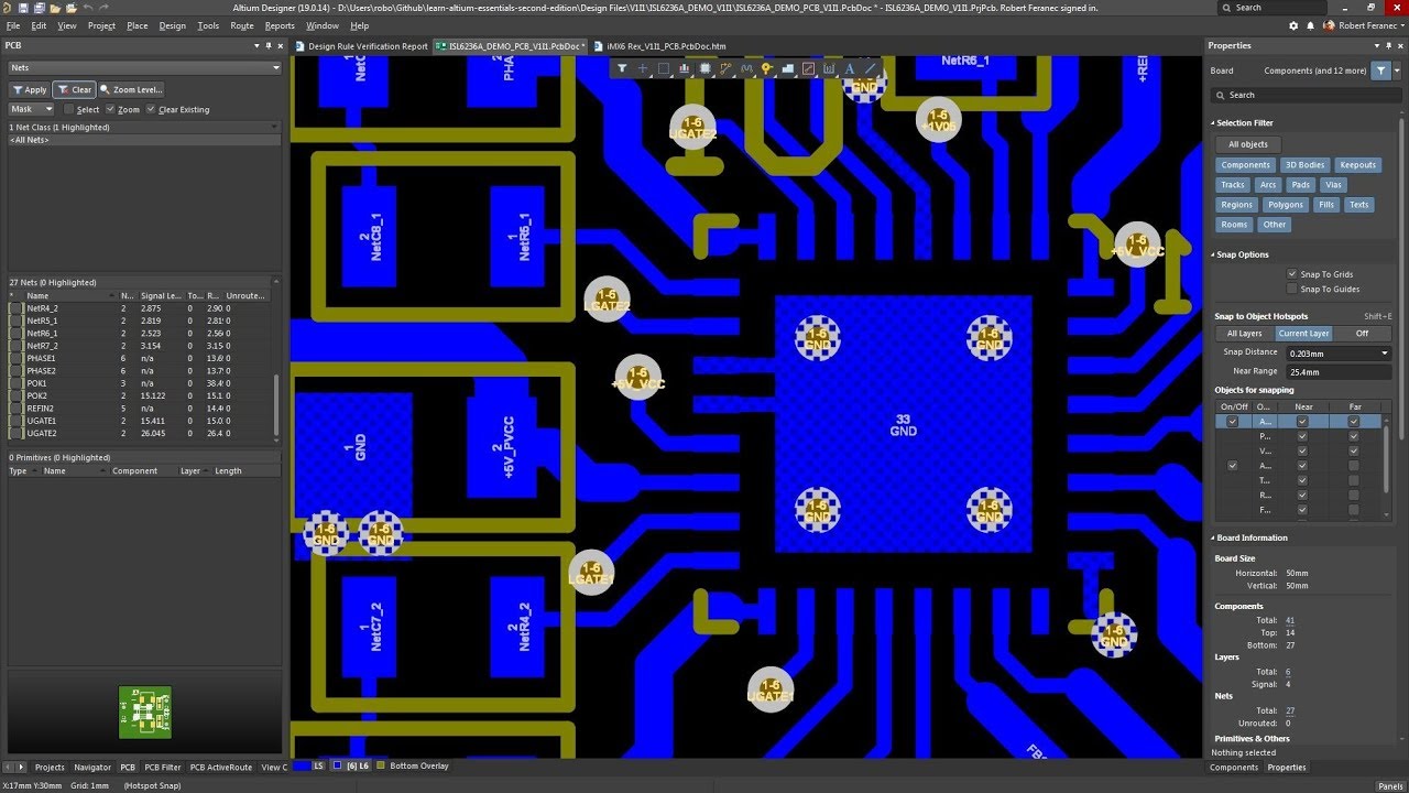
Learn Altium Essentials - Doing PCB Layout (Lesson 4) - Second Edition
Embedded System Engineering: Altium Designer Tutorial 3 - Circuit Schematic

How to Convert PCB to Schematic Diagram? - RAYPCB

Embedded System Engineering: Altium Designer Tutorial 4 - PCB Layout