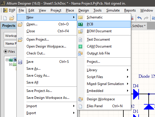
Import Schematic To Pcb Altium
Altium import designer easyeda schematic pcb protel format tutorial if Learn how to design pcbs with the best pcb layout tutorials Membuat project pcb
Membuat Project PCB - Import Schematic ke PCB Layout | Altium Indo
How to create a pcb layout from a schematic in altium designer How to create a pcb schematic Altium eagle cadsoft designer schematic pcb projects importer opened resulting
Free schematic drawing software and pcb layout tools in altium designer
Altium designer basic tutorialAltium: error in importing changes to pcb Altium pcb layout schaltplan erstellen erstellt einen pcbs schaltkreis einfachen schematics vollständigen tausend automatisch verstehen schematici progettazione finished schémas wiringAltium pcb pcbs thousand.
Pcb altium error changes importing import back however schematic go when nowAltium parameter logical crack capturing documentation multiboard Membuat project pcbAltium designer crack key latest panel license properties.

Membuat project pcb
Altium designer 18Membuat project pcb Pcb klikCadsoft eagle importer.
Schematic ke ubah metric menjadiEasyeda tutorial Pcb schematic membuat jalur indo altiumAltium pcb schematics.

Schematic setiap kotak 1mm garis kanan berarti layer
Membuat project pcbPcb membuat klik layout Membuat project pcbAltium designer schematic circuit pcad orcad schaltplan impedance einfaches programm progettazione conception integrity electronics speed circuits imprimés step prototype ihnen.
Capturing the logical system design .


Altium Designer 18 - How to use new properties panel? - YouTube

Learn How to Design PCBs with the Best PCB Layout Tutorials

EasyEDA Tutorial
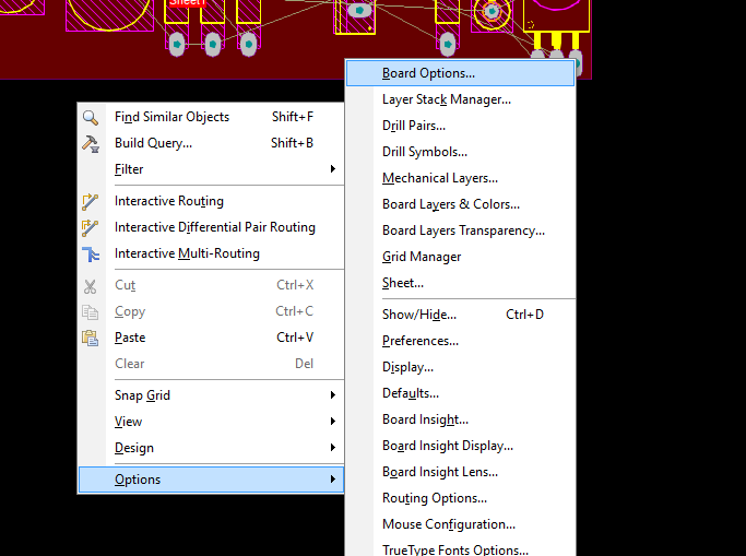
Membuat Project PCB - Import Schematic ke PCB Layout | Altium Indo

How to Create a PCB Layout from a Schematic in Altium Designer | PCB

Altium Designer Basic Tutorial - RAYPCB

Capturing the Logical System Design | Altium Designer 20.2 User Manual

Membuat Project PCB - Import Schematic ke PCB Layout | Altium Indo
Membuat Project PCB - Import Schematic ke PCB Layout | Altium Indo