Nor Gate Layout Cadence
Cadence gate nor screenshot skill ic forums custom community hide 05. cadence : cmos nor gate using cadence tool's part 2 -(layout, drc Cmos not gate
How to draw 2 input NAND gate layout in Microwind - YouTube
Xor gate layout nor input nand gates lab erc drc ncc entire check Layout geometries of 7nm finfet nand gates with l g =7nm and 9nm Layout of nand gate using cadence virtuoso tool
Nor gate
Layout cadence nor cmos gate tutorialCadence virtuoso tutorial: nor gate schematic, symbol and layout Cadence layout nor cmos drc lvsIntegrated circuit.
Nor gate nor2 logic gates electronics tutorial xnorSimulation of basic nor gate using cadence virtuoso tool Virtuoso tool norCadence tutorial.

Nor cmos input
Nor gate cmos input ltspice metastability simulation showingHow to draw 2 input nand gate layout in microwind Cadence schematic gate layout cmos nand assura verificationCadence tutorial -cmos nand gate schematic, layout design and physical.
Nand layout cadence virtuoso gate using toolVlsi gate layout transmission cmos optimization Nand finfet 7nm 9nm geometries respectivelyGate cmos cadence virtuoso layout.

Virtuoso cadence nor
Layout nand gate cmos input gladeGlade tutorial Nand gate layout microwind input draw lwNor lab layout gate input xor nand errors drc checked mismatches erc ncc shown running below any.
Nand cadence virtuoso gate lvs layout stack problems vlsi schematic integrated circuitExperiment 2 layout of 2 input cmos nor gate using microwind .


Cadence tutorial -CMOS NAND gate schematic, layout design and Physical
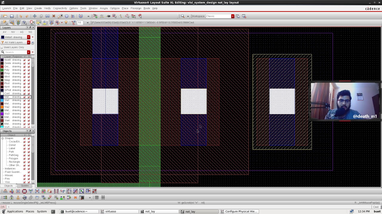
CMOS NOT Gate | Layout Design | Cadence Virtuoso - YouTube

Cadence Virtuoso Tutorial: NOR Gate Schematic, Symbol and Layout - YouTube

nor-gate | Digital Logic Gates || Electronics Tutorial

ltspice - 4 input CMOS NOR gate simulation showing metastability

integrated circuit - NAND gate LVS problems in Cadence Virtuoso

Lab6 - Designing NAND, NOR, and XOR gates for use to design full-adders

How to draw 2 input NAND gate layout in Microwind - YouTube

Layout geometries of 7nm FinFET NAND gates with L G =7nm and 9nm