Schematic Of And Gate
Gate diagram xor circuit sponsored links Conversion of nand gate to basic gates Gate nand nor xnor circuit vhdl xor logic simulate verify circuits wiring engineersgarage
Designing OR Gate Circuit using Transistor
(a) schematic of the gate driver with the short-circuit protection. (b Gate valve types and parts Xor cmos truth
Gate input circuit gates logic diagram sample multiple output operation digital led allaboutcircuits
Digital logic nor gate(universal gate)Nand gate nmos logic transistor schematic using digital universal ic symbols its two given below Understanding and logic gateGate valve types parts.
Transistor decompression decoderHandout on circuits and logic Gate xor logic exclusive schematic digital combinational sop inputReverse-engineering a vintage or/nor chip.

Digital logic nand gate(universal gate),its symbols & schematics
7432 integrated logic input ttl 74ls32 scavengerDesigning or gate circuit using transistor Or gate circuit diagram using ic 74ls32Circuit gate diagram ic pinout logic gates circuits input nand chip working diagrams circuitdigest electronic limitations these information voltage explanation.
Xor logic gates nand nor transistor inverter complex truthDiagram schematic gate circuit gates sponsored links Multiple-input gatesCmos logic circuits prevent does purpose schematics.

Gate logic schematic
Nand gates basic circuit electronicGate nor pmos schematic logic digital using series ic its two universal given below And gate circuit diagram & working explanationDesigning or gate circuit using transistor.
Gate logic ttl transistors diagram diodes electronics understanding technology method making digital source stackXor gate Gate logic gates symbol bbc circuit schematic bitesize note input basic truth gcse table circuits handout placed circle above electronicsVerilog code for 4:1 multiplexer (mux).

Welcome to real digital
Schematic diagram of and gateDiagram circuit logic gate gates ic schematic truth table using wiring circuits led electronic symbols Gate transistor using circuit diagram improved schematic designing circuits versionWhat is gate valves.
Exclusive-or (xor) digital logic gateScavenger's blog: or gate And gate transistor level schematicVerilog multiplexer rtl mux 4x1.

What does the and gate do to prevent electrical current?
Circuit diagram of xor gateGate transistor using circuit diagram schematic simple designing resistor simplest sharing two circuits emitter paralleled followers common Vhdl tutorial – 5: design, simulate and verify nand, nor, xor and xnor.
.


Digital Logic NOR Gate(Universal Gate) - All About Engineering

Conversion of NAND gate to Basic gates

Digital Logic NAND Gate(Universal Gate),Its Symbols & Schematics

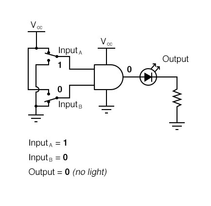
Understanding AND logic gate - Electrical Engineering Stack Exchange

Verilog code for 4:1 Multiplexer (MUX) - All modeling styles

AND Gate Circuit Diagram & Working Explanation
Multiple-input Gates | Logic Gates | Electronics Textbook